Final Project
APK Modem
by
prepared for
December 9, 1996
1. Abstract:
In today's ever-shrinking world, faster, more reliable digital communication via phone line or radio transmission is becoming more and more a necessity. For an electrical engineer dealing with digital communications or digital signal processing in any form, a solid understanding of the concepts behind these devices, known as modems (short for modulator/demodulator) is necessary. While many different versions of modulation/demodulation schemes exist in the market place, phase shift keying (PSK) as well as amplitude shift keying (ASK) are common examples. The combination of both these modulation schemes leads to very high data packing capability. For instance, a two level amplitude modulation of one frequency allows 1 bit of data to be sent per time period. Separately, PSK can also send 1 bit of data per time period by means of a 180° phase shift. The hybrid form of these two modulation/demodulation schemes doubles the transmission/reception rate of data per time period and is the focus of this project. In addition, full duplex transmission/reception and Motorola's EVM/DSP56002 host port B to PC bi-directional parallel port issues are addressed.
2. Introduction:
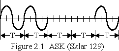 In general, modems can be categorized as having anywhere from one to three basic modulation types: amplitude modulation, frequency modulation, and phase modulation. While amplitude modulation is not commonly used by itself in modems, it is a simple addition to either phase or frequency modulation. The general form of amplitude modulation is:
 ,
,
where ai has a different value for each symbol being transmitted (Sklar 131). When combined with an FSK or a PSK modulation scheme, it can increase the number of bits per second (bps) transmitted on a fixed baud rate modem. Bits per second and baud rate are related by:
(baud rate)(symbol size) = bps ;
where the symbol size is simply the number of bits transmitted per period, T. T is the time period in which exactly one symbol may be transmitted. The number of levels increases exponentially with the symbol size. Because binary data is being transmitted, symbol size and levels are related by:
2 symbol size = levels .
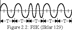 The Bell type 103 modem was one of the earliest modems in the marketplace. It consisted of a frequency shift keying (FSK) modulator/demodulator that operated on 1070Hz (space - 0), 1270Hz (mark - 1) in one direction, and 2025Hz (space), 2225Hz (mark) in the opposite direction. This modem was capable of transmitting two levels per symbol (1 bit of data) at up to 300 bits per second (bps) or 300 baud (Gibson 200). The general form of FSK modulation is:
 ;
;
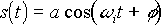
where  and a are fixed, and
  has the same number of discrete values as 2 raised to the power of the size of the symbol (Sklar 130). In the case of the 300 baud modem, can be two discrete frequencies.
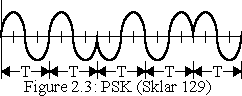 The phase shift keying modulation scheme, or PSK, is more common in recently designed modems. It is based on the premise that symbols may be distinguished from one another by the phase shift of one frequency. The general form of the PSK modem is:
 ;
;
where a and  are fixed and
  is 2 symbol size discrete values (Sklar 130).
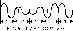 Of particular interest is the combination of the PSK and ASK modulation schemes. The combination of these two allows for greater symbol depth than each one individually. For instance, given an ASK modulation scheme capable of a symbol size of 1 and a PSK modulation scheme also capable of a symbol size of 1, this yields a combined symbol size of 2. The general form of the APK (amplitude phase keying) modem is as follows:
 ;
;
where is held constant but both ai and vary according to symbol (Sklar 131).
3. Analysis:
This project combines a two level PSK (symbol size of 1), also known as BPSK (binary PSK) with a two level ASK (symbol size of 1) to form a four level APK (symbol size of 2) modem.
In the modulation scheme, amplitude values are half and full values of the maximum output of the DSP56002 evaluation board. As in standard BPSK, 0° and 180° phase shifts are used. See the table below for the specific translation between amplitude/phase and binary value.
Bit
Representation |
Amplitude
Scaling |
Phase
Shifting |
| 00 |
full |
0° |
| 01 |
full |
180° |
| 10 |
half |
0° |
| 11 |
half |
180° |
Demodulation of the sampled signal, s(k), requires a rotating correlation filter in which the coefficients are synchronized during a negotiation phase to the dibit 00, and then rotated with the samples. 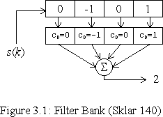 These coefficients are periodically re-synchronized throughout transmission. This allows for direct correlation between each of the sampled values and the filter coefficients. Using a single bank of filters synchronized to a 00 implies that a positive correlation yields a match of no phase shift (0 degrees or a 0 in the LSB), while a negative correlation is a 180 degree phase shift (a 1 in the LSB). Thus, the least significant bit (LSB) is determined. The magnitude of the correlation supplies the information required for the decoding of the most significant bit (MSB). A high amplitude corresponds with a 0, while a low magnitude yields a 1. The block diagram shows a sampled input, s(k), entering a shift register, called the correlation register, of depth 4. Each cell of the correlation register is synchronized with the incoming signal during transmission of 00 by simply copying a scaled input value to the appropriate cell of the shift register. This is preferred over defining discrete constants for the filter coefficients due to the fact that the signal will not likely perfectly coincide with these filter coefficients. By taking these samples directly, it is guaranteed that they will match. The correlation registers multiply with their corresponding filter coefficient and are all accumulated to determine the magnitude and sign of the current input signal.
4. Algorithm:
This modem is full-duplex and capable of two different modes: ORIGINATE or ANSWER. For either mode, the modem resides in one of three different phases throughout execution: negotiation_tx, negotiation_rx, or txrx. For the ORIGINATE modem, it enters phase 1 until a 00 response is received from the ANSWER modem. It then jumps to phase 2 and constructs its filter coefficients before moving on to phase 3 where it sends and receives data. The ANSWER modem starts in phase 2 transmitting an output power of 0dB (this is not a 00 dibit, but rather no power). It stays in this phase until the filter coefficients are built, at which point the modem moves to phase 3, where it also transmits and receives data. These three phases are described in detail below.
The main_event_loop always begins by receiving and storing a sample before checking its current phase. It then jumps to one of the three modes described above. The first is negotiation_tx, which is for the ORIGINATE modem only. This phase begins by calling the check_pwr subroutine which computes an L2 Norm, determining if any signal is being transmitted. If there is power, then the state is set so phase 2 will be entered the next time a sample is taken. Regardless, it continuously transmits a 00 dibit so the ANSWER modem can construct its filter coefficients. Transmission is accomplished by calling the subroutine produce_sample, which produces a 00 dibit sample, followed by a call to transmit_sample. This process is repeated until a mode change occurs by jumping to the beginning of the main_event_loop.
If phase 2 is set, then the modem enters the negotiation_rx state. In order to maintain compatibility with both the ORIGINATE and ANSWER modems, check_pwr is called. If this is the ORIGINATE modem, it receives power since the ANSWER modem has constructed its filter coefficients and while doing so transmits 00; however, it will not respond with start bits (i.e. phase 3) until it has fully constructed its own filter coefficients. If this is the ANSWER modem, it remains quiet in phase 2 until it has received 00 from the ORIGINATE modem (check_pwr). Then it fills its filter bank, responds with a 00 dibit, and allows the ORIGINATE modem to do the same. After both modems are ready, they move on to phase 3 for data transmission and reception for the remainder of execution.
Phase 3, txrx, begins with a call to filter_bits, where the signed magnitude of the current dibit being received is returned. This value is determined by macing (multiplying and accumulating) the filter coefficients with their corresponding samples. Decode_decision makes use of this correlation value and determines, by size of magnitude (greater or less than MAG_THRESH) and sign (positive or negative), the corresponding dibit, which is stored in a circular buffer for later use. Returning to the main_event_loop, if this dibit is a 00, then the filter coefficients are overwritten by the corresponding samples. This keeps the two modems synchronized; this is necessary due to slight differences in individual EVM56K clocks. Frame_decoder is called, which waits for a start dibit and counts out 4 data dibits (1 byte) worth of information. During the decoding of the individual dibits, the parity counter is also updated. The parity and stop dibit (stop bit is always 0) are received, and reception is suspended another start bit is found. Note that this is all done over many samples, after each returning to the main_event_loop. When decoding is complete, it is stored in memory or transmitted through the host port.
The other part of the full-duplex modem is the transmission of data simultaneously during phase 3. Frame_encoder is called to prepare the data in memory for transmission. It creates a frame of 12 bits: 2 start bits (11), 8 data bits (xx xx xx xx), 1 stop bit and 1 parity bit (x0). Splitting the frame into 6 dibits, each of which are passed through encode_dibits, whereby being converted to a sampled signal. This signal is then used by transmit_signal to send data to the other modem. Again, the whole process (reception and transmission) is repeated.
In the case that the hostport mode is enabled, the EVM performs an ACKnowledge/INItialize handshake with a PC via the EVM's host port B and the PC's bi-directional parallel port. Following this, the EVM places 8 bits of data on the host port and waits for the PC's STRobe signal to acknowledge reception of this data byte. Note that this occurs only when new data is received, and after transmission, the frame_out pointer is reset to overwrite old data.
5. Implementation Issues:
There are two basic components in any modem design: the transmitter and the receiver. Although these two are interdependent due to transmission/reception specifications such as frame and frequency, they can be designed individually and are described below.
Both the transmitter and receiver need to operate at the same speed, or same number of samples per cycle. This number is determined by the sampling frequency divided by the BAUD rate. With the BAUD rate set to 600 and a sampling rate of 9600 Hz, this yields an interval rate of 16 samples per cycle, or a data rate of (2)(600) = 1200bps (see introduction section for derivation).
Design of the transmitter:
A tone can be generated by selecting samples from the 256 entry sine-table found in ROM on the DSP evaluation board. These samples are chosen by using an offset into this table created by summing some  , where -1 < < 256, with the previous offset. Figure 3.1 shows a filter depth of 4, which implies 4 samples per cycle should be used from the sine-table. In other words, should be 1/4 of the table length. Therefore, having 256 samples in ROM yields = 64. Thus, at a sampling rate of 9600 Hz, a frequency of 2400 Hz is generated:
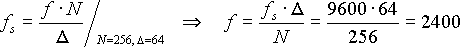 .
.
It is important to note that the must result in an integer number of samples per cycle. This is necessary since the correlation filter is of size and cannot contain fractional amounts of memory.
This tone is sent to the analog output port so the other modem can receive it. Since this is a stereo board, full-duplex can be achieved by sending outputs from the ORIGINATE modem on the left channel and the ANSWER modem on the right. Notice at this point it is irrelevant what the tone is; hence, this generic tone will be called the base signal and the filter coefficients of the other modem will be derived from this signal during the negotiation phase. The base signal, as a reference, will be decoded as a 00 dibit.
Alteration of the magnitude and/or phase is accomplished by taking the analog signal created by the routine above and performing an arithmetic shift accumulator right (asr) to halve the magnitude of the sample and/or by negating the accumulator for a 180° phase shift. Therefore, encoding a 11 takes the base signal, shifts it right to get a 10, and then negates it.
Because of the asynchronous nature of this modem, some method is required to signal the beginning and ending of transmission. This can be done by taking data and prefixing with start bits and suffixing with a stop bit. This sequence, or frame, is constructed with one start dibit of 11, followed by the data which resides in memory (one byte = 4 dibits), and ends with the parity check and stop bit (0) together forming the 6th dibit of the frame.
Design of the receiver:
For the receiver to work properly, it must have a filter bank which holds enough values to decode the input signal correctly. Since is 64, there are 4 different samples per full cycle (64 is one-quarter of the entire number of samples in ROM: 256); therefore, 4 samples are used as the length of the filter bank. This filter bank is initially filled in the negotiation mode by buffering the previous four samples and saving them.
Transition states arise when changing from one dibit to a different dibit. During transition, dibit values may be interpreted which should not exist in the data stream. In these cases it is still necessary to determine the value that the other modem was intending to send. This is achieved by storing out the current decision and the previous three decoded decisions and comparing all four decisions. If all four are equal, then the decision is accepted and that value is stored in memory as prev_dibit for other subroutines to use. However, if the four decisions are not all equal, the value at prev_dibit remains unchanged.
recv_correlation
| 00 |
01 |
10 |
11 |
| 00 |
01 |
10 |
11 |
| 00 |
01 |
10 |
11 |
| 00 |
01 |
10 |
11 |
| 00 |
04 |
40 |
44 |
The test for equality between all four decoded values is rather unique. The current and previous samples are stored in a circular queue known as recv_correlation. The binary dibit values are stored at nybble boundaries, meaning a 11 binary (3 hex) is stored as 11 hexadecimal. All four correlation values are summed. If the result of this summation does not contain a 0 or 4 in both positions, then the signal is invalid and prev_dibit will be used instead.
To decode a data stream into information, it must be interpreted as a frame. Therefore, the receiver waits until a start dibit is seen (11) in prev_dibit. Once there, the receiver waits an additional 4 samples to make sure the signal is smooth and then resets the interval counter to the sampling frequency divided by the BAUD rate. This counter decrements until zero is reached, at which time it restores the data portion from memory and shifts it left two places, to make room for the next incoming data dibit. Then it resets the counter and or's the current dibit with the previous data. It also decrements a dibit counter, which was initialized to 5. Once the dibit counter has reached zero, the y memory location frame_out will contain the correct data.
The parity and stop bit section is next, which stores this dibit into a y memory location following the respective data. Since the stop bit is always a 0, the 11 dibit guarantees a change. Execution will remain in this state, regardless of time, until these bits are seen. This allows for any mistakes in the interval counter (possibly due to the different speeds of the two clocks) to be compensated for and corrected.
Due to variations in clocks from one modem to the next, the receiver must also re-synchronize its filter coefficients. For every 00 dibit that is decoded, this re-synchronizing process is executed. This code merely takes a snapshot of the values in recv_queue and copies them directly to recv_filter. It then resets the pointers correctly and continues execution. By synchronizing every few dibits, the probability that the clocks never get far enough off to lose data is greatly increased.
The hostport data transmission code was originally taken from Motorola's SPEC.ZIP spectrograph demonstration code and was greatly shortened and optimized. Cable schematics and other board jumper settings can be found in this zip archive in SPEC2.DOC.
In general, the transmit and receive code for either the ORIGINATE or ANSWER mode is approximately 1000 lines of assembly code, plus an additional 60 lines of Borland C (version 2.0) code to implement the parallel hostport connection on the PC.
6. Testing:
Each major phase of transmitter design was manually tested thoroughly using an oscilloscope. The oscilloscope allowed debugging of problem areas, primarily in the transmitter. In particular, the original design for the transmitter was to increment the offset pointer for the sine-table (n4) by half of the number of coefficients in this ROM table, thus creating a 180° phase shift. However, the results on the scope showed a "flow" of the sine waves that were generated. Instead of changing phase at the axis, as shown in Figure 2.3 or 2.4, the phase changes were occurring at different points along the sine wave. In order to resolve this, the tone was generated as if it should be a 00 dibit, and then it was negated to create the phase shift. Looking again at the scope shows that this algorithm is sound. However, for implementing more phase shifts than two (BPSK), this problem must be further considered.
Another problem area was the difference in clock speeds between two EVM boards. Running the program via a loop-back cable on a single board enabled a sampling rate of 16 KHz at a frequency of 4 KHz, for a total of 4000bps. The program was executed for more than 10 minutes without any data loss. However, when combined with another EVM, problems arose. First, the sampling rate, frequency, and BAUD rate had to be reduced to 9.6 KHz, 2.4 KHz, and 600 BAUD respectively. More importantly, received data became corrupted after approximately 500 samples, due to losing signal correlation. This led to the design of a re-synchronization subroutine. Every time a 00 signal is transmitted, the filters re-synchronize themselves to the previous values stored in recv_queue. This code was again tested and was also found to transmit flawlessly for at least 10 minutes.
The last item implemented was the parallel port communication between the host PC and the EVM. The supplied SPEC2.C file was used as a base, but was highly modified. The modified version takes incoming, decoded data and displays it to the screen. The limiting factor in this routine is the speed at which communication between the video card and the C code takes place. After the first round of modifications to the C code, there existed the problem of the monitor not displaying all the characters. It was determined that the access was too long; consequently, the C code was optimized, removing all unnecessary lines. On the next trial, it displayed correctly until the characters reached the bottom of the page and needed to scroll up. Here, correlation was almost completely lost. Since the C code had already been optimized, it was determined that the video card was unable to handle the speed at which it was receiving data. Hence, the video card was swapped with a faster one and the result was perfect. This code displayed data to the monitor for more than 3 and a half hours without a mistake.
7. References:
Sklar, Bernard. Digital Communications: Fundamentals and Applications.
Prentice Hall: Englewood Cliffs, 1988.
Gibson Jerry D. Principles of Digital and Analog Communications.
Macmillan Publishing Company: New York, 1989.
SPEC.ZIP. Semiconductor Products Sector, Digital Signal Processing Division.
8. Appendix